
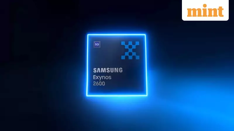
Samsung Electronics has taken a monumental leap in mobile chipset technology with the official launch of the Exynos 2600. This new high-end system-on-chip (SoC) is set to be the powerhouse behind select flagship Galaxy smartphones, anticipated to debut early next year, most likely starting with the Galaxy S26 series. The announcement marks a pivotal moment in Samsung's in-house semiconductor development, showcasing its ambition to lead in advanced chip manufacturing.
The 2nm GAA Process: A Foundational Leap
At the core of the Exynos 2600's innovation is its manufacturing process. Samsung has built this chip using its own Foundry's cutting-edge 2-nanometer Gate-All-Around (GAA) node technology. This makes it the world's first smartphone processor to utilize a 2nm process. The shift to this advanced node is engineered to deliver significant improvements in both raw performance and energy efficiency compared to chips built on older processes. Samsung has integrated the CPU, GPU, and NPU into a single, compact package, with a pronounced emphasis on accelerating artificial intelligence tasks and delivering top-tier gaming experiences.
Powerful Core Architecture and AI Enhancements
The Exynos 2600 features Samsung's proprietary eight-core CPU design, a configuration tailored for balanced and powerful performance. The setup includes:

- One ultra-high-performance C1-Ultra core, clocked at speeds up to 3.8GHz.
- Three C1-Pro cores running at 3.25GHz.
- Four additional C1-Pro cores operating at up to 2.75GHz.
A key advancement is the CPU's support for ARM's Scalable Matrix Extension 2 (SME2) instruction set, specifically designed to speed up AI and machine learning workloads. Samsung claims this architectural enhancement results in up to a 39 percent boost in CPU computing performance while simultaneously improving power efficiency.
Advanced Graphics, AI Processing, and Thermal Management
For graphics, Samsung is deploying the Xclipse 960 GPU. This deca-core solution, based on the ARMv9.3 architecture, promises major gains for mobile gamers. The company states it offers up to 50 percent better ray tracing performance than the GPU in the previous Exynos 2500. On the artificial intelligence front, the dedicated Neural Processing Unit (NPU) boasts a 32K MAC capability, enabling Samsung to claim that generative AI performance has more than doubled over its predecessor. The chip also incorporates Exynos Neural Super Sampling technology, which uses AI for resolution upscaling and frame generation to enhance in-game visuals.
Addressing a common concern in high-performance chips, Samsung has introduced a new thermal solution dubbed "Heat Pass Block." This technology optimizes the internal heat transfer path within the chip, reportedly reducing thermal resistance by up to 16 percent and offering heat dissipation comparable to a traditional heat sink.
Comprehensive Support for Flagship Features
The Exynos 2600 is built to support the premium specifications expected in next-generation smartphones. It will enable devices with:
- LPDDR5x RAM and UFS 4.1 storage.
- Displays with resolutions up to 4K or WQUXGA and refresh rates of up to 120Hz.
- Advanced camera systems, including support for a single 320-megapixel sensor or a dual-camera setup of 64MP + 32MP.
- High-resolution video capabilities, such as 108MP recording at 30fps and 8K video recording and playback at 30 frames per second.
The unveiling of the Exynos 2600 solidifies Samsung's commitment to competing at the highest level of mobile silicon. With its pioneering 2nm process, focused AI improvements, and robust gaming features, the chip is poised to set a new benchmark for performance and efficiency in the flagship Android segment when it arrives in Galaxy devices early next year.