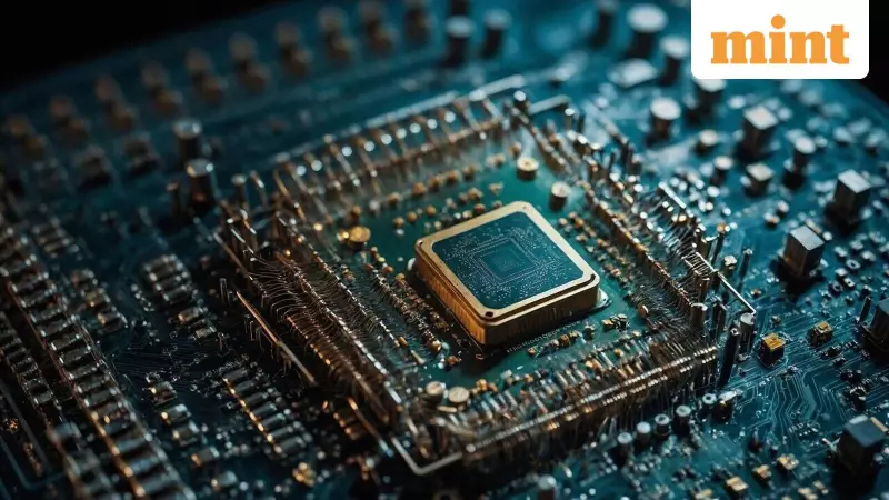
In a significant boost to India's semiconductor ambitions, Union Electronics and Information Technology Minister Ashwini Vaishnaw revealed on Tuesday that Tata Electronics' upcoming semiconductor fabrication plant in Dholera, Gujarat, will join the state-owned Semiconductor Laboratory (SCL) in Mohali in providing crucial tape-out support to domestic chip-design startups. This development marks a pivotal step toward building a self-reliant semiconductor ecosystem within the country.
What is Tape-Out and Why It Matters for Indian Startups
Tape-out refers to the critical phase when a chip's final design is submitted to a semiconductor fabrication facility, or fab, which then prepares it and produces the first physical prototype chips for rigorous testing. Currently, numerous Indian startups are forced to depend on overseas fabs, such as Taiwan Semiconductor Manufacturing Company (TSMC) and US-based GlobalFoundries, to obtain even limited samples of their chips before mass production can commence.
This reliance on foreign facilities is not only costly but also severely hampers the ability of Indian startups to conduct essential failure analysis, testing, and firsthand identification of manufacturing or assembly challenges. The logistical and financial burdens associated with overseas tape-outs have been a major bottleneck in the growth of India's semiconductor design industry.
Building a Domestic Fabrication Ecosystem
Minister Vaishnaw, speaking at an industry event in New Delhi, elaborated on the strategic importance of this initiative. "The second facility, which will be used for taping-out, will be Tata's Dholera fab. So the Dholera fab - 28 nanometer (nm) to 90 nm and SCL's 180 nm. In a sense, close to 75-80% of the kind of chips which are manufactured in the world. That entire ecosystem we will be able to build in our country within the next 2-3 years," he stated confidently.
The minister's announcement came during a meeting with 24 chip-design firms selected under the government's Design Linked Incentive (DLI) scheme. He noted that 14 of these startups have already secured venture capital funding totaling approximately ₹430 crore, indicating growing investor confidence in the sector.
Current Limitations and Future Upgrades
Presently, the SCL Mohali facility supports chip-design startups and academic institutions with tape-outs, but it operates on an outdated 180-nm technology node, which restricts work on more advanced projects. In a move to address this limitation, the government announced in November a comprehensive modernization plan for SCL Mohali, involving an investment of ₹4,500 crore over three years.
A government official, speaking on condition of anonymity, revealed that tape-outs for academic chip designs are primarily conducted at SCL on a multi-project wafer (MPW) basis. However, startups that have progressed to the tape-out stage typically utilize TSMC's facilities, for which they receive incentives under the DLI scheme.
Industry Perspectives and Government Vision
Arumugam Govindswamy, Managing Director of MBit Wireless, a fabless semiconductor company specializing in cellular Internet of Things (IoT) technology, welcomed the development. "Tata's Dholera plant for tape-outs will certainly support the startup ecosystem building products in 28 nm and 40 nm technology. The price points for tape-outs, however, should not be higher than the global rates. Then it will be beneficial," he emphasized.
Govindswamy further highlighted that the key demands from the industry for the next phase of the chip design scheme include increased funding for tape-outs and mass production, alongside improved market access for selling finished semiconductor products.
Long-Term Semiconductor Roadmap
Separately, Minister Vaishnaw outlined an ambitious long-term vision for India's semiconductor industry. The government aims to achieve the capability to manufacture and design high-tech chips at the 3-nanometer node by 2032, which are essential for cutting-edge products like modern smartphones and computers. The roadmap even envisions progressing to 2-nm technology in the future.
"The level of 2032 is to reach 3 nanometer chips manufacturing and design. Design, of course, we are doing even today. But manufacturing, we should reach 3 nanometer," the minister declared. He added optimistically that in the coming years, 50% of all global semiconductor design work could be conducted in India.
Focus Areas and Startup Targets
Under the second phase of the DLI scheme, the government will concentrate on six specific categories of chips: compute, radio frequency, networking, power, sensor, and memory. Vaishnaw announced a target of nurturing 50 fabless startups in this next phase, reinforcing the commitment to expanding India's design capabilities.
"As we go into 2029, we will have a major capability of manufacturing and designing the chips which are required practically in 70-75% of all applications in our country," the minister projected, underscoring the strategic goal of import substitution and technological self-sufficiency.
Incentive Structure and Startup Challenges
The current DLI scheme offers selected startups a subsidy of up to ₹15 crore. Additionally, there are deployment-linked incentives for startups that successfully reach the commercial sales stage, offering 4-6% of net sales (capped at ₹30 crore per application). However, no startup has yet claimed these deployment-linked incentives, as none have progressed to the deployment phase.
During the meeting with the minister, several startups appealed for enhanced market access for their chip products and increased funding support. This request is particularly critical as they transition into the mass production phase following tape-out, a stage that involves substantial financial outlays and operational complexities.
The integration of Tata's Dholera fab into India's semiconductor infrastructure represents a transformative step. By providing domestic tape-out capabilities alongside SCL Mohali, it promises to reduce costs, accelerate development cycles, and foster innovation among Indian chip startups, ultimately contributing to the nation's strategic and economic objectives in the global semiconductor arena.


