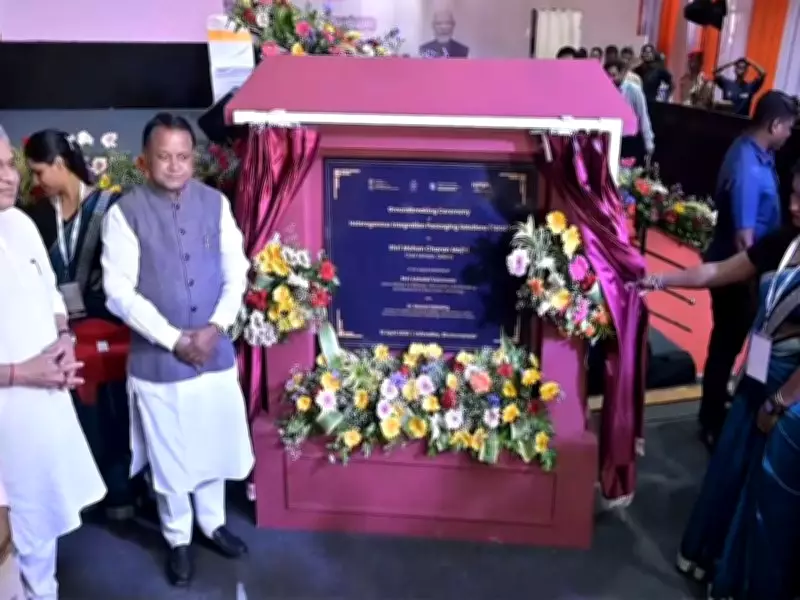
3D Glass Solutions Announces Major Investment in Odisha for Advanced Chip Packaging
In a significant development for India's semiconductor industry, 3D Glass Solutions has unveiled plans to invest a substantial Rs 1,943 crore in Odisha. This investment is earmarked for the establishment of a state-of-the-art advanced chip packaging facility, with the ambitious goal of commencing production by the year 2030. The move underscores a strategic push to enhance domestic capabilities in the critical semiconductor sector, aligning with national initiatives to reduce dependency on imports and foster technological self-reliance.
Details of the Investment and Facility
The Rs 1,943 crore investment by 3D Glass Solutions represents a major commitment to Odisha's industrial landscape. The advanced chip packaging facility will focus on cutting-edge technologies essential for modern electronics, including 3D integration and glass-based packaging solutions. These technologies are pivotal for improving performance, reducing power consumption, and enabling miniaturization in devices such as smartphones, automotive systems, and IoT applications. The facility is expected to create numerous high-skilled jobs and stimulate local economic growth, positioning Odisha as a key player in India's semiconductor manufacturing ecosystem.
Strategic Importance and Production Timeline
This investment is strategically timed to capitalize on the global semiconductor shortage and India's renewed focus on boosting domestic production. By targeting a production start date of 2030, 3D Glass Solutions aims to align with the government's vision under schemes like the Production Linked Incentive (PLI) for semiconductors. The facility will not only cater to domestic demand but also potentially serve export markets, enhancing India's competitiveness in the global tech arena. Experts highlight that advanced packaging is a crucial link in the semiconductor value chain, often overlooked but vital for innovation and cost-efficiency.

Impact on India's Semiconductor Ecosystem
The establishment of this facility is poised to have a ripple effect across India's semiconductor ecosystem. It will:
- Strengthen Supply Chains: Reduce reliance on foreign suppliers for advanced packaging, mitigating risks associated with geopolitical tensions and supply disruptions.
- Boost R&D: Foster research and development in materials science and engineering, driving innovation in glass-based and 3D packaging technologies.
- Attract Further Investments: Signal confidence in India's semiconductor potential, potentially drawing more companies to invest in similar ventures across the country.
Industry analysts note that this move by 3D Glass Solutions could catalyze a broader transformation, making India a hub for semiconductor manufacturing and packaging in the coming decade.