India's Semiconductor Dream: A Strategic, Step-by-Step Path Forward
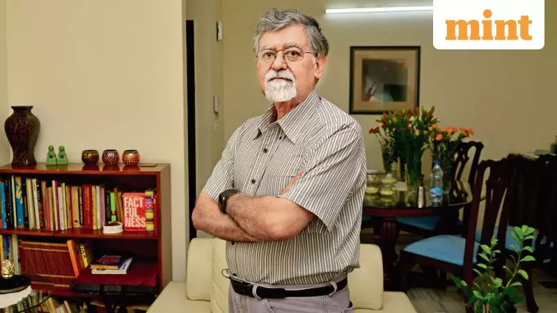
According to prominent economist and NITI Aayog member Arvind Virmani, India's aspiration to become a global semiconductor powerhouse requires a meticulously planned, long-term approach focused on ecosystem development. Virmani stresses that achieving substantial domestic semiconductor capacity is not an overnight endeavor but a gradual process demanding sustained investment in research and development alongside collaborative governance.
Government Collaboration and Policy Instruments
Virmani underscores the critical need for the Central and state governments to work in unison. Building a robust semiconductor ecosystem necessitates carefully crafted policy instruments, with subsidies being the most straightforward tool, alongside significant improvements in the ease of doing business. He highlights that ensuring essential infrastructure—such as reliable land, high-quality water, and uninterrupted electricity—for investors is paramount and falls largely under state government purview.
"State governments are very important given the need for land, water, power, etc., which have to be made available. Semiconductor facilities require high-quality water and reliable electricity. All that has to be provided at the state level. Otherwise, it will not work," Virmani explained.
The Role of Free Trade Agreements and Anchor Investors
Virmani points to the proposed India-European Union Free Trade Agreement (FTA) as a potential game-changer. He believes this pact can attract anchor investors from sectors like semiconductors, bringing with them established global supply chains and ready markets. This integration eliminates the need for Indian businesses to independently seek market access, embedding them directly into the global value chain.
"I see huge potential in the India-EU FTA," Virmani stated, adding that such an investor brings an entire supply chain, which is crucial as they already possess the market. He cited the example of Apple's iPhone contract manufacturing and exports from India as a successful model.
EY India partner Saurabh Agarwal echoed this sentiment, noting that the FTA could be a defining moment for India's industrial landscape. "By integrating European R&D in electrolyzers and offshore wind with India’s engineering scale, we can position our country as the global nerve centre for green hydrogen and circular EV ecosystems. This partnership, if concluded in a time-bound manner, may act as a catalyst for our semiconductor ambitions," Agarwal said.
Building the Ecosystem Step-by-Step
Virmani advocates for a phased development strategy, acknowledging that no single nation can produce every component in the complex semiconductor value chain. This reality underscores the importance of cultivating trusted international partnerships.
"You have to create the semiconductor ecosystem step-by-step. No single nation can produce every ingredient or sub-component. That underscores the importance of trusted partners, because in network products, every small component works together as a whole," he elaborated.
He explained that countries typically begin with basic assembly and testing before gradually developing parts of the value chain. This process allows companies to connect with others possessing specific expertise, thereby fostering the domestic ecosystem. However, he cautioned that semiconductor core technologies are highly specialized, making the journey more challenging and necessitating a patient, incremental approach distinct from smaller nations.
Current Landscape and Government Initiatives
India's current semiconductor scenario reveals a heavy reliance on imports, with annual domestic consumption estimated at over $50 billion and no large-scale commercial fabrication plant yet operational. In response, the government has launched the India Semiconductor Mission in December 2021, backed by a substantial ₹76,000-crore outlay. This initiative offers:
- Fiscal support of up to 50% of project cost for semiconductor fabrication plants (fabs)
- Support for display units, packaging, and chip design facilities
- Production-Linked Incentive (PLI) schemes for electronics manufacturing
Several approved projects, including wafer fabs and assembly and testing units, are under implementation and expected to establish initial domestic production capacity in the coming years.
The Strategic Imperative
Virmani connects semiconductor capability directly to India's stature as a major global economy in the information age. Today's investments in R&D are crucial, as they will position India to accelerate to the technological and manufacturing frontier in about a decade. Prime Minister Narendra Modi's emphasis on self-reliance and the mission to build 10 new semiconductor units underscores this national priority.
"In the information age, semiconductors go into everything, and they are an important part of being a major global economy. But it's a step-by-step process," Virmani concluded, framing the semiconductor journey as a collaborative, strategic marathon essential for India's economic and technological sovereignty.


