Elon Musk Announces Groundbreaking Terafab Semiconductor Project
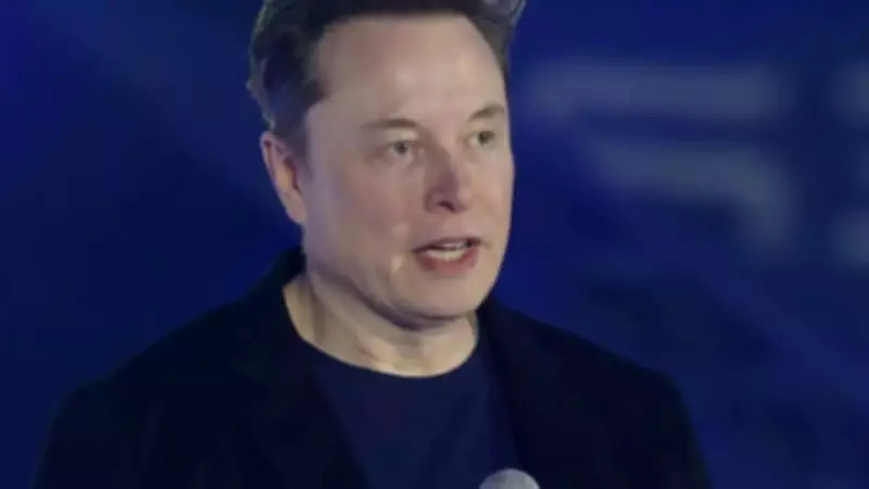
In a major technological announcement, Elon Musk has revealed plans for a massive semiconductor production facility named "Terafab," to be developed jointly by Tesla Inc. and SpaceX. The announcement was made in Austin on March 21, 2025, marking a significant step toward in-house chip manufacturing for Musk's companies.
What is the Terafab Project?
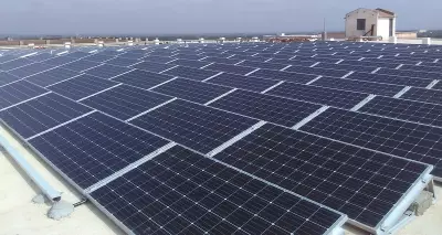
Terafab is a large-scale semiconductor manufacturing plant designed to produce critical components for artificial intelligence hardware, automotive chips, and advanced computing systems. The facility aims to address the growing market demand for these components while eliminating dependence on external suppliers.
According to Musk, the plant will serve long-term purposes for both terrestrial and space-based computing, supporting artificial intelligence systems and satellite networks. This strategic move comes as global demand for semiconductors continues to surge across multiple industries.

Unprecedented Scale and Production Capacity
The proposed Terafab facility is expected to dwarf existing semiconductor plants in size. During the launch event, Musk indicated the total area could reach approximately 100 million square feet, making it substantially larger than current chip manufacturing facilities.
The plant is designed for high-volume semiconductor wafer production, with capacity intended to support between 100 and 200 gigawatts of computing power annually for Earth-based systems. Additionally, the facility may contribute to space-based computing with potential output reaching 1 terawatt per year under one roof, as mentioned in SpaceX's social media posts.
Strategic Location and Development Status
The project is currently in early development stages, with multiple locations under consideration. While initial attention focused on areas near Gigafactory Texas in Austin, Musk clarified that only a smaller chip design facility would be located there. The primary manufacturing operations will require a separate, significantly larger site.
In a social media post on March 22, 2026, Musk confirmed the project's distributed location strategy, with separate sites for design and manufacturing operations. The facility requires thousands of acres of land and won't fit within existing Tesla facilities.
Core Features and Technological Significance
The Terafab project represents several key technological advancements:
- Scale and Infrastructure: The 100 million square foot facility will be one of the world's largest semiconductor plants
- Production Output: Designed to support massive computing capacity for AI platforms, robots, and satellite data centers
- Strategic Supply Chain: Aims to secure semiconductor supply for Tesla vehicles, Optimus robots, and SpaceX operations
- Space Integration: Supports development of orbital data centers requiring high-performance chips for AI workloads
Project Timeline and Future Outlook
The Terafab project remains in early planning stages, with construction of the main manufacturing facility yet to begin. Initial hiring efforts are underway as the companies evaluate potential locations. Musk described the project with enthusiasm, stating "This will be one hell of a building!"
The facility represents a significant investment in vertical integration for Musk's companies, potentially transforming how they source critical computing components while advancing both Earth-based and space-based technological capabilities.