
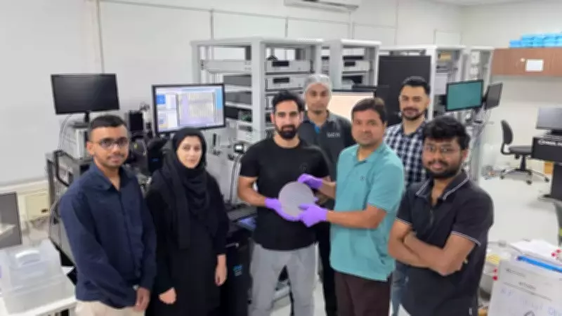
IISc Researchers Achieve Major Breakthrough in Gallium Nitride Power Transistor Technology
Scientists from the Indian Institute of Science (IISc) in Bengaluru have announced a significant advancement in the design of gallium nitride (GaN) power transistors, a development poised to accelerate the adoption of this superior material across critical sectors including electric vehicles, data centers, and renewable energy infrastructure.
The Promise and Challenge of Gallium Nitride
Gallium nitride is widely recognized as the successor to silicon in high-power electronic applications due to its exceptional ability to drastically reduce energy losses and shrink the physical size of power converters by nearly threefold. Despite these advantages, widespread commercial implementation has progressed cautiously due to inherent reliability limitations in existing device architectures.
"Existing GaN devices typically utilize a p-GaN gate structure that activates at a relatively low threshold voltage, approximately 1.5 to 2 volts," explained the IISc team. "Beyond 5 to 6 volts, these devices begin to experience current leakage, which critically undermines their reliability in demanding, high-performance applications." This fundamental constraint has hindered the full potential of GaN technology.

Unraveling the Physics Behind Device Behavior
To address this challenge, a dedicated research group from the Department of Electronic Systems Engineering at IISc embarked on a comprehensive two-part study to decode the underlying physics governing transistor operation. The investigation focused specifically on how the gate structure controls current flow and what determines the crucial threshold voltage.
Led by Professor Mayank Shrivastava, the team first established a critical connection between the depletion state of the p-GaN layer, the presence of microscopic leakage pathways, and the precise moment the transistor switches on. "Our research revealed that even minuscule leakage paths can decisively influence the entire turn-on behavior of the device," Professor Shrivastava noted, highlighting the sensitivity of these components.
Experimental Insights and Innovative Gate Design
The scientists conducted extensive experimentation, creating multiple gate variants and employing a combination of electrical measurements, advanced modeling, and microscopy techniques. Their analysis uncovered a key mechanism: when the p-GaN layer is only partially depleted, tiny electrical charges accumulating at a critical interface can prematurely trigger the device to switch on.
By developing methods to suppress this unwanted charge accumulation, the researchers successfully forced the transistor to activate at a later, higher, and significantly safer voltage threshold. Leveraging these insights, the IISc team engineered novel metal-based gate stacks that demonstrated a dramatic reduction in leakage current—by up to 10,000 times—while simultaneously enhancing the stability of the threshold voltage. These new designs achieved gate breakdown voltages of approximately 15.5 volts, representing a substantial improvement over current commercial offerings.
Patented Integrated Gate Stack and Practical Applications
In the second phase of their work, the researchers developed an integrated aluminium–titanium oxide gate stack, a patented concept that effectively blocks undesirable charge injection. This innovation enables a high-threshold operational mode comparable to traditional silicon MOSFET devices.
The resulting GaN transistors achieved threshold voltages exceeding 4 volts while maintaining excellent control characteristics and robust performance. "This advancement has the potential to significantly hasten the deployment of GaN technology in applications where reliability is paramount," stated Rasik Rashid Malik, the doctoral researcher and lead author of the study. Key application areas include:

- Electric Vehicle Power Converters
- High-Efficiency Server Power Supplies for data centers
- Advanced Inverters for solar and other renewable energy systems
Path Forward for Commercialization and Industry Impact
The IISc team is now actively pursuing avenues to scale this promising technology through strategic government support and industry partnerships. Professor Shrivastava emphasized that achieving a combination of high threshold voltage and low leakage current was essential for the next major phase of GaN adoption in the global electronics sector.
"Our work directly addresses a long-standing technical barrier that has limited the reliability and performance of gallium nitride power devices," he added. "By providing a pathway to more stable and efficient transistors, we are contributing to the foundation for next-generation power electronics that will drive sustainability and technological progress." This breakthrough positions Indian research at the forefront of a critical materials science frontier with far-reaching implications for energy efficiency and electronic innovation worldwide.