
Bengaluru: India's semiconductor ambitions received a major boost after the Odisha government signed an MoU with Intel and US-based 3DGS on Friday to bring advanced substrate manufacturing technology to the country. The Centre described the initiative as one of India's largest high-technology manufacturing investments.
Project Details
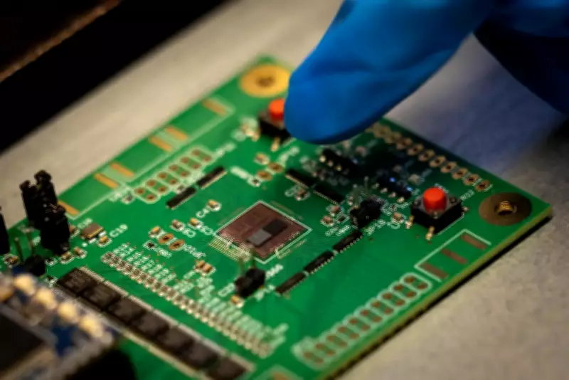
The project, estimated at around $3.3 billion, will set up an advanced packaging glass-core substrate manufacturing facility in the Bhubaneswar-Khurda region of Odisha. The proposed unit will focus on advanced packaging glass-core substrates, high-density interconnect substrates and related semiconductor technologies.
Key Signatories
Union electronics and IT minister Ashwini Vaishnaw, Odisha chief minister Mohan Charan Majhi, Intel CEO Lip-Bu Tan and other dignitaries witnessed the signing of the agreement. Vaishnaw said investments by global semiconductor firms reflect growing confidence in India's semiconductor push and the government's policy efforts in the sector.

"Congratulations to the Government of Odisha, Intel and 3DGS on signing an MoU to bring substrate manufacturing technology to India. This will further advance the semiconductor ecosystem in India," the Union minister wrote on X.
Employment and Implementation
The project will be implemented in phases over five to six years and is expected to create more than 1,800 direct high-skilled jobs, besides generating indirect employment opportunities across manufacturing and technology ecosystems.
Strategic Importance
The Centre said the initiative builds on efforts under the India Semiconductor Mission (ISM) to strengthen domestic manufacturing, semiconductor design capabilities and supply-chain resilience. Substrates are a critical component in semiconductor packaging, helping connect and support semiconductor chips used in electronic devices. Industry executives have often described substrate manufacturing as one of the missing links in India's semiconductor value chain.
Broader Ecosystem
The latest development adds to India's broader semiconductor ecosystem push, which has already seen companies such as Applied Materials, Lam Research and Tokyo Electron announce investments or partnerships in the country. The government has also been pushing semiconductor packaging and assembly capabilities alongside chip fabrication projects.
Earlier this month, the government approved two semiconductor-related projects under the ISM. These include a gallium nitride-based mini/micro LED display facility and a semiconductor packaging unit in Gujarat involving investments of around Rs 3,936 crore.
The Odisha project is expected to support export-oriented manufacturing and position the state as an emerging semiconductor and digital infrastructure hub.