IISc Researchers Achieve Breakthrough in Growing Ultra-Thin Magnetic Materials at Scale
In a significant advancement that could pave the way for smaller and more efficient electronic devices, researchers from the Indian Institute of Science (IISc) in Bengaluru have successfully developed a method to grow ultra-thin magnetic materials over large surfaces. This development marks a crucial step toward real-world applications of these materials in next-generation electronics.
What Are 2D Magnetic Materials?
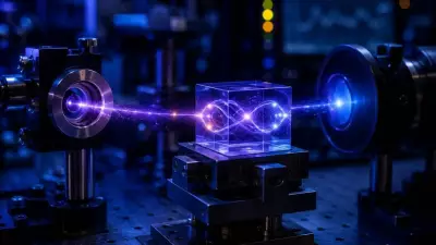
These materials, known as 2D magnetic materials, are only a few atoms thick yet retain their magnetic properties. This unique characteristic makes them highly valuable for a range of devices, including hard drives, sensors, and emerging spintronics technologies. Spintronics relies on the spin of electrons rather than their charge, offering potential for more energy-efficient computing and data storage solutions.
Overcoming Previous Limitations
Until now, scientists could only produce these materials in tiny flakes, which severely limited their practical use in commercial electronics. The IISc team, led by assistant professor Akshay Singh, has overcome this hurdle by developing a technique to grow these materials across centimetre-scale wafers, similar to those used in semiconductor chip manufacturing. Their groundbreaking work has been published in the prestigious journal Advanced Materials.

Innovative Growth Technique: Physical Vapour Transport Deposition
Instead of relying on the traditional method of peeling thin layers from bulk material—a process suited only for laboratory experiments—the team employed a technique called Physical Vapour Transport Deposition (PVTD). In this method, the material is first vaporized and then allowed to settle as a thin film on a surface. The primary challenge was to ensure the material formed evenly without defects, as even minor disturbances can compromise its magnetic properties.
Key Modifications to the Process
To address this, the researchers implemented several critical modifications:
- Reduced excess heat and light inside the growth chamber to minimize disturbances.
- Pushed carrier gas flow rates far beyond conventional levels to enhance uniformity.
- Carefully controlled the supply of material during growth to prevent inconsistencies.
- Removed oxygen and moisture from the environment, as these elements can damage the sensitive materials.
Optimal Surface Selection and Transfer Capability
A key finding of the research was the choice of surface. After testing various options, the team discovered that synthetic mica worked best, allowing the material to form smooth, well-ordered layers. Additionally, the researchers successfully transferred these films onto other surfaces, a vital step for integrating them into electronic devices such as chips and sensors.
Broader Implications for Technology
The IISc team believes this method can be extended to other sensitive materials, opening up new possibilities for advanced electronic and data storage technologies. This breakthrough could accelerate the development of ultra-compact, high-performance devices, contributing to innovations in computing, telecommunications, and beyond.
This research underscores India's growing role in cutting-edge scientific advancements and highlights the potential for transformative impacts on global technology landscapes.