
Odisha to Host India's First Advanced 3D Glass Semiconductor Packaging Unit
Bhubaneswar, the capital city of Odisha, is set to become the home of India's first advanced 3D glass semiconductor packaging unit. Chief Minister Mohan Charan Majhi will lay the foundation stone for this groundbreaking Rs 1,943 crore project on Sunday, marking a significant milestone in India's technological advancement.
Breakthrough for India's Semiconductor Ecosystem
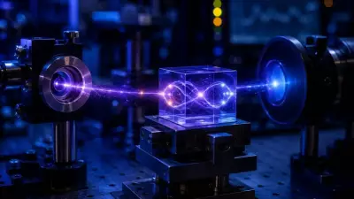
The facility will be established by Heterogeneous Integration Packaging Solutions, also known as 3D Glass Solutions. This project represents a major breakthrough for India's chip ecosystem by introducing one of the most sophisticated packaging technologies currently available worldwide. The state government has emphasized that this initiative will bring advanced chip packaging technology to India for the first time.
The project is expected to create approximately 2,500 jobs while significantly strengthening Odisha's position in the global semiconductor landscape. Once operational, the plant at Info Valley will have the capacity to produce an impressive 50 million assembled units annually, adding substantial scale to India's semiconductor value chain.

Strategic Importance and Commercial Value
The packaged chips produced at this facility will serve several critical sectors including aerospace, defense, artificial intelligence, 5G technology, and data centers. This diverse application base gives the project strong commercial value while simultaneously supporting India's strategic push to build domestic strength in crucial technologies.
With this new unit, Odisha becomes the first state in India to host both a compound semiconductor fabrication facility and an advanced 3D chip packaging plant using glass substrates. This dual capability reflects Odisha's growing semiconductor ecosystem and its successful efforts to attract high-technology investment.
Rapid Implementation and Government Support
The state's electronics and IT department noted that the foundation ceremony is taking place just months after receiving Union Cabinet approval, highlighting the remarkable pace of execution. This rapid implementation demonstrates the government's commitment to advancing India's semiconductor capabilities.
The project aligns perfectly with the larger Atmanirbhar Bharat vision by promoting advanced manufacturing and technology-based employment. Odisha is strategically positioning itself to emerge as a leading destination for semiconductor and electronics investment in India.
High-Profile Inauguration
The foundation stone laying ceremony will be attended by Union Electronics and IT Minister Ashwini Vaishnaw and Electronics and IT Minister Mukesh Mahaling, along with senior government officials, industry leaders, investors, and academic representatives. This high-level participation underscores the national importance of this semiconductor initiative.
This development represents a significant step forward in India's journey toward semiconductor self-reliance and technological sovereignty. The 3D glass packaging technology represents the cutting edge of semiconductor manufacturing, positioning Odisha at the forefront of next-generation semiconductor manufacturing and packaging capabilities in India.